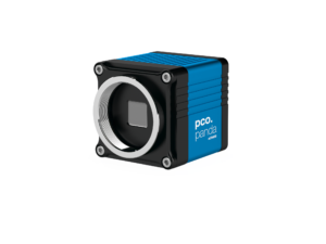
Description
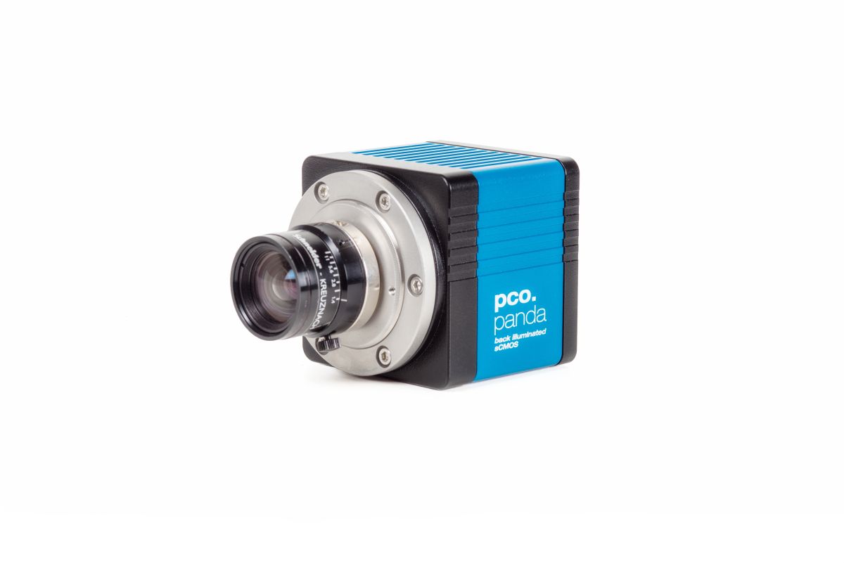
PCO’s new, unique pco.panda 4.2 bi UV has been specially developed to make working in the ultraviolet wavelength range whilst benefiting from the latest sCMOS sensor technology possible for the first time.
The specialised input window inside the camera achieves high QE in the ultraviolet wavelength range. The system itself is based on PCO’s compact pco.panda series with modern back illuminated sensor technology. This makes the camera perfect for demanding lighting conditions, even without active cooling.
The high resolution and 6.5 x 6.5 μm² pixel size guarantees users greater detail diversity and high quality images. The USB 3.1 interface provides direct power delivery via the USB cable. PCO’s latest developments in sCMOS technology and compact dimensions make the pco.panda 4.2 bi UV ideal for countless applications in microscopy and life science.
Key Features:
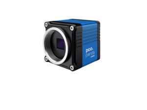
- ultra-compact size: 65 x 65 x 65 mm³
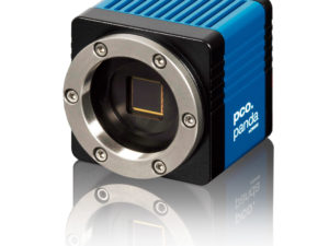
- back illuminated 16 bit sCMOS sensor technology
- high resolution 2048 x 2048 pixel
- pixel size: 6.5 x 6.5 µm²
- quantum efficiency up to 95 %
- exposure times from 100 µs to 1 s
- maximum frame rate 40 fps @ full resolution
- rolling shutter
- USB 3.1 Gen1 interface
- power over USB
Quantum Efficiency Curve:

View/ Download the datasheet here.
Area Applications:
- brightfield microscopy
- fluorescence microscopy
- digital pathology
- single molecule localization microscopy
- lightsheet fluorescence microscopy (LSFM)
- calcium imaging
- FRET
- FRAP
- structured illumination microscopy (SIM)
- high-speed bright field ratio imaging
- high throughput screening
- high content screening
- biochip reading
- TIRF microscopy
- spinning disk confocal microscopy
- 3D metrology
- ophthalmology
- industrial quality inspection
Application Example:
SMLM DNA Origami
 DNA origami is a powerful method for the programmable assembly of nanoscale molecular structures. For applications of these structures as functional biomaterials, the study of reaction kinetics and dynamic processes in real time and with high spatial resolution becomes increasingly important. Read more here.
Thin Film Analysis with pco.edge 4.2 bi UV
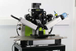
Ellipsometry is a non-destructive, optical technique for surface characterization. It probes a sample by shining in polarized electromagnetic radiation at an oblique angle of incidence, with photon energies typically being in the range from the ultraviolet up to the infrared part of the electromagnetic spectrum. Ellipsometry in general detects any change of the probing beam’s polarization ellipse – hence the name “ellipsometry” – that may occur upon its reflection from the sample surface. Such a change is introduced by almost any thin film covering the sample surface and thus, one of the main applications of ellipsometry is to determine the layer thickness of thin films in a range of typically 0.1 nm up to 20 µm.
Imaging Ellipsometry in particular combines traditional ellipsometry with optical microscopy and thus enables ellipsometric studies with a lateral resolution down to 1 µm. Therefore, it is perfectly suited to study structured or very small samples such as MEMs, FETs, Biochips or flakes of 2D-Materials.
Recently there has been an increasing interest in high-power electronics using wide bandgap semiconductors like silicon carbide (SiC), gallium nitride (GaN) and others. In order to characterize those materials it is important to probe the sample with electromagnetic radiation whose photon energy is higher than the bandgap of the material. As shorter wavelengths feature higher photon energies, it is favorable to perform ellipsometric studies at wavelengths as short as possible.
As the leading producer of imaging ellipsometers, Accurion GmbH (Göttingen, Germany) has been using CCD and CMOS camera technology for more than 20 years. With respect to the UV range, up to now, their products were limited by the lack of suitable, scientific-grade, high-sensitivity, low-noise detectors and thus studies were only possible down to 250 nm using sophisticated back-thinned CMOS cameras.
The appearance of the pco.edge 4.2 bi UV changed the situation completely. Being a low-light application, imaging ellipsometry especially benefits from the very high sensitivity and extremely low noise level of the sCMOS technology. Combined with the fact that the pco.edge 4.2 bi UV additionally features a very good response in the ultraviolet spectrum of light it was, for the first time, possible to build an imaging ellipsometer operating in the wavelength range of 190 nm up to 1000 nm.
The imaging ellipsometer EP4 is a modular device which can be equipped with a multitude of light sources, detectors and sample handling systems. Studies are possible on small samples as well as wafers of up to 300 mm in diameter.